How to Prevent Another Europa Clipper Transistor Panic
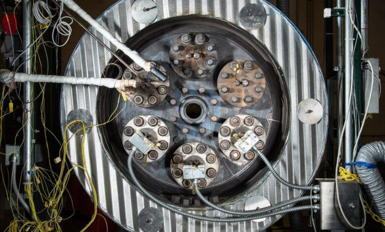
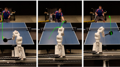
Yesterday, NASA successfully launched the Europa Clipper, the largest spacecraft the agency has ever built for a planetary mission. Clipper is now successfully on its multi-year journey to Europa, bristling with equipment to study the Jovian moon’s potential to support life—but just a few months ago, the mission was almost doomed. In July, researchers at NASA found out that a group of Europa Clipper’s transistors would fail under Jupiter’s extreme radiation levels. They spent months testing devices, updating their flight trajectories, and ultimately adding a warning “canary box” to monitor the effects of radiation as the mission progresses.
The canary box “is a very logical engineering solution to a problem,” says Alan Mantooth, an IEEE Fellow and a professor of electrical engineering at the University of Arkansas. But ideally, it wouldn’t have been needed at all. If NASA had caught the issues with these transistors earlier or designed their circuits with built-in monitoring, this last minute scramble wouldn’t have occurred. “It’s a clever patch,” says Mantooth, “but it’s a patch.”
Scientists have been “radiation hardening” electronics—designing them to function in a radioactive environment—since the 1960s. But as missions to space become more ambitious, radiation hardening techniques have had to evolve. “It’s kind of like cybersecurity,” says Mantooth. “You’re always trying to get better. There’s always a more harsh environment.”
With the rapid acceleration of companies like SpaceX, the space industry is at “a massive inflection point,” says Eric Faraci, an engineer at Infineon who works on aerospace and defense projects. “Everything we used to take for granted about how you do something, what’s accepted, best practices—everything’s been questioned.”
In future space exploration, we’ll see more systems made with alternative semiconductors like silicon carbide, specialized CMOS transistors, integrated photonics, and new kinds of radiation-resistant memory. Here’s your guide to the next generation of radiation hardened technology.
Silicon Carbide’s Ultra Wide Band Gap
Most power devices in spacecraft today use silicon as the semiconductor, but the next generation will use silicon carbide, says Enxia Zhang, a researcher at the University of Central Florida who has been developing radiation hard microelectronics for over 20 years. Silicon carbide is more resistant to radiation because of its wider band gap, which is the extra energy electrons need to transition from being bound to an atom’s nucleus to participating in conduction. Silicon has a band gap of 1.1 electron volts, while silicon carbide’s ranges from 3.3 to 3.4 eV. This means that more energy is required to disturb an electron of silicon carbide, so it’s less likely that a dose of stray radiation will manage to do it.
Silicon carbide chips are being manufactured right now, and NASA holds a weekly meeting to test them for space missions, says Zhang. NASA’s silicon carbide devices are expected to be used on missions to the Moon and Venus in the future.
“People are flying silicon carbide” devices right now, says Infineon’s Faraci. They are getting around a lack of standards by using them at parameters well below what they are designed for on Earth, a technique called derating.
Another semiconductor with a suitably wide band gap is gallium nitride (3.2 eV). Most commonly found in LEDs, it is also used in laptop chargers and other lower power consumer electronics. While it’s a “very exciting” material for space applications, it’s still a new material, which means it has to go through a lot of testing to be trusted, says Faraci.
Gallium nitride is best suited for cold temperatures, like on Mars or the dark side of the Moon, says Mantooth. But “if we’re doing something on Mercury or we’re doing something close to the Sun—any high temperature stuff … silicon carbide’s your winner.”
Silicon on Insulator Designs and FinFETs for Designing Radiation-Hardened CMOS
New materials aren’t the only frontier in radiation hardening; researchers are also exploring new ways of designing silicon transistors. Two CMOS production methods are already have a radiation hardened form: silicon on insulator (SOI), and fin field effect transistors (FinFETs). Both methods are designed to prevent a kind of radiation damage called single event effects, where a high energy particle hits an electronic device, jolting its electrons into places they shouldn’t be and flipping bits.
In ordinary bulk CMOS, current flows from the source to the drain through the channel, with a gate acting as a switch, blocking or allowing the current’s flow. These sit in the top layer of silicon. Radiation can excite charges deeper down in the silicon bypassing the gate’s control and allowing current to flow when it shouldn’t. Radiation hardening methods work by impeding the movement of these excited electrons.
SOI designs add a layer of an insulator like silicon oxide below the source and the drain, so that charges cannot flow as easily below the channel. FinFET designs raise the drain, source, and the channel between them into one or more 3D “fins”. Excited charges now have to flow down, around, and back up in order to bypass the gate. FinFETs are also naturally resistant to another form of radiation damage: the total ionizing dose, which occurs when a slow buildup of charged particles changes the properties of the insulating layer between the channel and gate of a device.
The techniques to produce SOI devices and FinFETs have existed for decades. In the 2000s, they weren’t used as much in radiation hardening, because circuit designers could still use ordinary, bulk CMOS devices, mitigating radiation risks in their circuit design and layout, according to Hugh Barnaby, a professor of electrical engineering at Arizona State University. But lately, as CMOS devices have gotten smaller and therefore more vulnerable to radiation, there’s been renewed interest in producing these naturally radiation hard varieties of CMOS devices, even if they are more specialized and expensive.
Barnaby is working with a team on improving radiation hardness in FinFETs. They found that adding more fins increased the device’s ability to control current, but reduced its radiation hardness. Now they are working to rearrange where the fins are to maximize the effectiveness of radiation resistant circuits. “We haven’t done this quite yet,” says Barnaby, “but I’m sure it will work.”
Photonic Systems for High Bandwidth, Faster Data Transfer
Photonic systems use light instead of electrons to transfer information over long distances with little energy. For example, the Internet uses optical fibers to quickly transfer large amounts of data. Within the last decade, researchers have developed silicon photonics integrated circuits which are currently used for high bandwidth information transmission in data centers, but would also enable us to move high volumes of data around in spacecraft, according to John Cressler, a professor of electronics at Georgia Tech.
“If you think of some of the systems that are up in space, either maybe they’re remote sensing or communication,” says Cressler, “they have a lot of data that they’re gathering or moving and that’s much easier to do in photonics.”
The best part? Photonics integrated circuits are naturally radiation hard, because their data transfer is done using photons instead of electrons. A high energy dose of radiation won’t disrupt a photon as it would an electron, because photons are not electrically charged.
Cressler anticipates that integrated photonics will be used in spacecraft in the next two years. “NASA and the [U.S. Department of Defense] and even commercial space [companies] are very interested in photonics,” he says.
Nonvolatile Memory in Space
Another promising area of research for radiation hardness in space is new kinds of nonvolatile memory. Computers usually use static random access memory (SRAM) or dynamic random access memory (DRAM). These are volatile memories, which means once the power is off, they cannot store their state. But nonvolatile memories are able to remember their state. They don’t require continuous power, and therefore reduce power consumption needs.
There are two front-runners in nonvolatile memory for use in space: Magnetoresistive-RAM (MRAM), and Resistive-RAM (ReRAM). MRAM uses magnetic states to store data, and ReRAM uses a quality called memristance. Both technologies are radiation hard simply by how they are designed; radiation won’t affect the magnetic fields of MRAM or the resistances of ReRAM.
“Resistive RAM is one of the technologies that has the potential to get to neuromorphic, low energy computing,” says Michael Alles, the director of the Institute for Space and Defense Electronics at Vanderbilt University, referring to a form of computing inspired by how brains work. Satellites usually are not equipped with the ability to process much of their own data, and have to send it back to Earth. But with the lower power consumption of memristor-based circuits, satellites could do computations onboard, saving communications bandwidth and time.
Though still in the research phases, Zhang predicts we will see nonvolatile memory in space in the next 10 to 15 years. Last year, the U.S. Space Force contracted Western Digital $35 million dollars to develop nonvolatile radiation hardened memory.
A Note of Caution and Hope
Alles cautions, however, that the true test for these new technologies will not be how they do on their own, but rather how they can be integrated to work as a system. You always have to ask: “What’s the weak link?” A powerful and radiation hard memory device could be for naught, if it depends on a silicon transistor that fails under radiation.
As space exploration and satellite launches continue to ramp up, radiation hardening will only become more vital to our designs. “What’s exciting is that as we advance our capabilities, we’re able to go places we haven’t been able to go before and stay there longer,” says Mantooth. “We can’t fly electronics into the Sun right now. But one day, maybe we will.”
IEEE Spectrum