Hybrid Bonding Plays Starring Role in 3D Chips
Researchers at the IEEE Electronic Components and Technology Conference (ECTC) last week pushed the state of the art in a technology that is becoming critical to cutting-edge processors and memory. Called hybrid bonding, the technology stacks two or more chips atop each other in the same package, allowing chipmakers to increase the number of transistors in their processors and memories despite a general slowdown in the pace of the traditional transistor shrinking that once defined Moore’s Law. Research groups from major chipmakers and universities demonstrated a variety of hard-fought improvements, with a few—including from Imec, Intel, and Sony—showing results that could lead to a record density of connections between 3D stacked chips of around 7 million links in a square millimeter of silicon.
All those connections are needed because of the new nature of progress in semiconductors, Intel’s Yi Shi told engineers at ECTC. As Intel general manager of technology development Ann Kelleher explained to IEEE Spectrum in 2022, Moore’s Law is now governed by a concept called system technology co-optimization, or STCO. In STCO, a chip’s functions, such as cache memory, input/output, and logic are separated out and made using the best manufacturing technology for each. Hybrid bonding and other advanced packaging tech can then reassemble them so that they work like a single piece of silicon. But that can only happen with a high density of connections that can shuttle bits between pieces of silicon with little delay or energy consumption.
Hybrid bonding is not the only advanced packaging technology in use, but it provides the highest density of vertical connections. And it dominated ECTC, making up about one-fifth of the research presented, according to Chris Scanlan, senior vice president of technology at Besi, whose tools were behind several of the breakthroughs.
“It’s difficult to say what will be the limit. Things are moving very fast” —Jean-Charles Souriau, CEA Leti
In hybrid bonding, copper pads are constructed at the top face of each chip. The copper is surrounded by insulation, usually silicon oxide, and the pads themselves are slightly recessed from the surface of the insulation. After chemically modifying the oxide, the two chips are then pressed together face-to-face, so the recessed pads align with each. This sandwich is then slowly heated, causing the copper to expand across the gap, connecting the two chips.
Hybrid bonding can either attach individual chips of one size to a wafer full of chips of a larger size or it can be used to bond two full wafers of chips of the same size together. Thanks in part to its use in camera chips, the latter is a more mature process than the former. Imec, for example, reported some of the most dense wafer-on-wafer (WoW) bonds ever with a bond-to-bond distance (or pitch) of just 400 nanometers. The same research center managed a 2-micrometer pitch for the chip-on-wafer (CoW) scenario. (Commercial chips today have connections about 9 micrometers apart.)
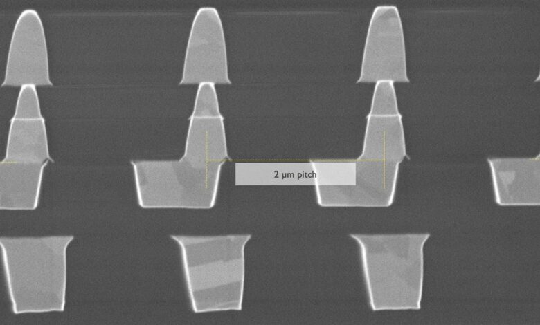
Hybrid bonding starts by forming recessed copper pads at the top of the chip [top]. The surrounding oxide dielectric bonds when the two chips are pressed together [middle]. Annealing expanding the copper to form a conductive connection [bottom].
“With the equipment available, it’s easier to align wafer to wafer than chip to wafer. Most processes for microelectronics are made for [full] wafers,” says Jean-Charles Souriau, scientific leader in integration and packaging at the French research organization, CEA Leti. However, it’s chip-on-wafer (or die-to-wafer) that’s making a splash in high-end processors such as AMD’s Epyc line, where the technique is used to assemble compute cores and cache memory in its advanced CPUs and AI accelerators.
In pushing for tighter and tighter pitches for both scenarios, researchers focused on making surfaces fractionally flatter, getting bound wafers to stick together better, and cutting the time and complexity of the whole process. Getting it right could ultimately mean enabling a revolution in how chips are designed.
WoW, those are some tight pitches
The wafer-on-wafer (WoW) research that reported the tightest pitches—500 nanometers to 360 nanometers—all spent a lot of effort on one thing: flatness. To bind two wafers together with 100-nanometer-level accuracy, the whole wafer has to be nearly perfectly flat. If it’s bowed or warped, whole sections of the materials won’t connect.
Flattening wafers is the job of a process called chemical mechanical planarization, or CMP. It’s key to chipmaking generally, especially for the parts of the process that produce the layers of interconnects above the transistors.
“CMP is a key parameter we have to control for hybrid bonding,” says Souriau. Results presented this week at ECTC took CMP to another level, not just flattening across the wafer, but reducing mere nanometers of roundness on the insulation between the copper pads to ensure better connections.
Other research focused on ensuring those flattened parts stuck together strongly enough by experimenting with different surface materials such as silicon carbonitride instead of silicon oxide or by using different schemes to chemically activate the surface. Initially, when wafers or dies are pressed together, they are held in place with relatively weak hydrogen bonds, and the concern is ensuring everything stays in place between the bonding and further steps. Bound wafers and chips are then heated slowly (a process called annealing) to form stronger chemical bonds. Just how strong these bonds are—and how to even figure that out—was the subject of a lot of research at ECTC.
Part of that final bond strength would come from the copper connections as well. The annealing step expands the copper across the gap to form a conductive bridge. Controlling the size of that gap is key, explained Samsung’s Seung Ho Ahn. Too much of a gap and the copper won’t connect. Too little and it will push the wafers apart. It’s a matter of nanometers, and Ahn reported research on a new chemical process that hopes to get it just right by etching away the copper a single atomic layer at a time.
The quality of the connection counts, too. Even after the copper expands, most schemes showed that the metal’s grain boundaries don’t cross from one side to another. Such a crossing reduces a connection’s electrical resistance and should boost its reliability. Researchers at Tohoku University in Japan reported a new metallurgical scheme that could finally generate large, single grains of copper that cross the boundary. “This is a drastic change,” said Takafumi Fukushima, an associate professor at Tohoku University. “We are now analyzing what underlies it.”
“I think it’s possible to make more than 20-layer stack using this technology” —Hyeonmin Lee, Samsung
Other experiments focused on streamlining the hybrid bonding process. Several sought to reduce the annealing temperature needed to form bonds—typically around 300 °C—motivated by the potential to reduce any risk of damage to the chips from the prolonged heating. And researchers from Applied Materials presented progress on a method to radically reduce the time needed for annealing—from hours to just 5 minutes.
CoWs that are outstanding in the field
Chip-on-wafer (CoW) hybrid bonding is more useful to industry at the moment: It allows chipmakers to stack chiplets of different sizes together, and it allows them to test each chip before it’s bound to another, ensuring that they aren’t fatally dooming an expensive CPU with a single flawed part.
But CoW comes with all of the difficulties of WoW and fewer of the options to alleviate them. For example, CMP is designed to flatten wafers, not individual dies. Once dies have been cut from their source wafer and tested there’s less that can be done to improve their readiness for bonding.
Nevertheless, Intel reported CoW hybrid bonds with a 3-micrometer pitch and Imec managed 2 micrometers, largely by making the transferred dies very flat while they were still attached to the wafer and keeping them extra-clean going forward. Efforts by both groups used plasma etching to dice up the dies instead of the usual method, which uses a specialized blade. Plasma won’t lead to chipping at the edges, which creates debris that interferes with connections. It also allowed the Imec group to shape the die, making chamfered corners that relieved mechanical stress that could break connections.
CoW hybrid bonding is going to be critical to the future of high-bandwidth memory (HBM), several researchers told IEEE Spectrum. HBM is a stack of DRAM dies atop a control logic chip—currently 8 to 12 dies high. Often placed within the same package as high-end GPUs, HBM is crucial to providing the tsunami of data needed to run large language models like ChatGPT. Today, HBM dies are stacked using so-called microbump technology, in which tiny balls of solder between each layer are surrounded by an organic filler.
But with AI pushing memory demand even higher, DRAM makers want to do 20 layers or more in HBM chips. However, the volume microbumps take up mean that these stacks will soon be too tall to fit in the package with GPUs. Hybrid bonding would not just shrink the height of HBMs, it should also make it easier to remove excess heat from the package, because there is less thermal resistance between its layers.
A 200-nanometer WoW pitch is not just possible, but desirable.
At ECTC, Samsung engineers showed that a hybrid bonding scheme could make a 16-layer HBM stack. “I think it’s possible to make more than 20-layer stack using this technology,” said Hyeonmin Lee, a senior engineer at Samsung.
Other new CoW technology could help bring hybrid bonding to high-bandwidth memory. Though they didn’t present research on this at ECTC, researchers at CEA Leti are working on so-called self-alignment technology, says Souriau. That would help ensure CoW connections using chemical processes. Some parts of each surface would be made hydrophobic and some hydrophilic, resulting in surfaces that would slide into place automatically.
At ECTC, researchers at Tohoku University and Yamaha Robotics reported work on a similar scheme, using the surface tension of water to align 5-micrometer pads on experimental DRAM chips with better than 50 nanometer accuracy.
How far can hybrid bonding go?
Researchers will almost certainly keep pushing the pitch of hybrid bonding connections. A 200-nanometer WoW pitch is not just possible, but desirable, Han-Jong Chia, a program manager pathfinding systems at TSMC, told engineers at ECTC. Within two years, TSMC plans to introduce a technology called backside power delivery. (Intel plans it for the end of this year.) That’s a technology that puts the chip’s chunky, power-delivery interconnects beneath the silicon instead of above it. With those out of the way, the uppermost interconnect levels can connect better to smaller hybrid bonding bond pads, TSMC researchers calculate. Back side power delivery with 200-nanometer bond pads would cut down the capacitance of 3D connections so much that the product of energy efficiency and signal delay would be as much as 8 times better than with 400-nanometer bond pads.
At some point in the future, if bond pitches are narrowed even further, Chia suggested, it might become practical to “fold” blocks of circuitry so they are built across two wafers. That way some of the longer connections within the block might be made shorter by the vertical pathway, potentially speeding computations and lowering power consumption.
And hybrid bonding may not be limited to silicon. “Today there is a lot of development in silicon-to-silicon wafers, but we are also looking to do hybrid bonding between gallium nitride and silicon wafers and glass wafers… everything on everything,” says CEA Leti’s Souriau. His organization even presented research on hybrid bonding for quantum computing chips, which involves aligning and binding superconducting niobium instead of copper.
“It’s difficult to say what will be the limit,” Souriau says. “Things are moving very fast.”
IEEE Spectrum