Tsunenobu Kimoto Leads the Charge in Power Devices
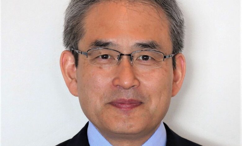
Tsunenobu Kimoto, a professor of electronic science and engineering at Kyoto University, literally wrote the book on silicon carbide technology. Fundamentals of Silicon Carbide Technology, published in 2014, covers properties of SiC materials, processing technology, theory, and analysis of practical devices.
Kimoto, whose silicon carbide research has led to better fabrication techniques, improved the quality of wafers and reduced their defects. His innovations, which made silicon carbide semiconductor devices more efficient and more reliable and thus helped make them commercially viable, have had a significant impact on modern technology.
Tsunenobu Kimoto
Employer
Kyoto University
Title
Professor of electronic science and engineering
Member grade
Fellow
Alma mater
Kyoto University
For his contributions to silicon carbide material and power devices, the IEEE Fellow was honored with this year’s IEEE Andrew S. Grove Award, sponsored by the IEEE Electron Devices Society.
Silicon carbide’s humble beginnings
Decades before a Tesla Model 3 rolled off the assembly line with an SiC inverter, a small cadre of researchers, including Kimoto, foresaw the promise of silicon carbide technology. In obscurity they studied it and refined the techniques for fabricating power transistors with characteristics superior to those of the silicon devices then in mainstream use.
Today MOSFETs and other silicon carbide transistors greatly reduce on-state loss and switching losses in power-conversion systems, such as the inverters in an electric vehicle used to convert the battery’s direct current to the alternating current that drives the motor. Lower switching losses make the vehicles more efficient, reducing the size and weight of their power electronics and improving power-train performance. Silicon carbide–based chargers, which convert alternating current to direct current, provide similar improvements in efficiency.
But those tools didn’t just appear. “We had to first develop basic techniques such as how to dope the material to make n-type and p-type semiconductor crystals,” Kimoto says. N-type crystals’ atomic structures are arranged so that electrons, with their negative charges, move freely through the material’s lattice. Conversely, the atomic arrangement of p-type crystals’ contains positively charged holes.
Kimoto’s interest in silicon carbide began when he was working on his Ph.D. at Kyoto University in 1990.
“At that time, few people were working on silicon carbide devices,” he says. “And for those who were, the main target for silicon carbide was blue LED.
“There was hardly any interest in silicon carbide power devices, like MOSFETs and Schottky barrier diodes.”
Kimoto began by studying how SiC might be used as the basis of a blue LED. But then he read B. Jayant Baliga’s 1989 paper “Power Semiconductor Device Figure of Merit for High-Frequency Applications” in IEEE Electron Device Letters, and he attended a presentation by Baliga, the 2014 IEEE Medal of Honor recipient, on the topic.
“I was convinced that silicon carbide was very promising for power devices,” Kimoto says. “The problem was that we had no wafers and no substrate material,” without which it was impossible to fabricate the devices commercially.
In order to get silicon carbide power devices, “researchers like myself had to develop basic technology such as how to dope the material to make p-type and n-type crystals,” he says. “There was also the matter of forming high-quality oxides on silicon carbide.” Silicon dioxide is used in a MOSFET to isolate the gate and prevent electrons from flowing into it.
The first challenge Kimoto tackled was producing pure silicon carbide crystals. He decided to start with carborundum, a form of silicon carbide commonly used as an abrasive. Kimoto took some factory waste materials—small crystals of silicon carbide measuring roughly 5 millimeters by 8 mm—and polished them.
He found he had highly doped n-type crystals. But he realized having only highly doped n-type SiC would be of little use in power applications unless he also could produce lightly doped (high purity) n-type and p-type SiC.
Connecting the two material types creates a depletion region straddling the junction where the n-type and p-type sides meet. In this region, the free, mobile charges are lost because of diffusion and recombination with their opposite charges, and an electric field is established that can be exploited to control the flow of charges across the boundary.
“Silicon carbide is a family with many, many brothers.”
By using an established technique, chemical vapor deposition, Kimoto was able to grow high-purity silicon carbide. The technique grows SiC as a layer on a substrate by introducing gasses into a reaction chamber.
At the time, silicon carbide, gallium nitride, and zinc selenide were all contenders in the race to produce a practical blue LED. Silicon carbide, Kimoto says, had only one advantage: It was relatively easy to make a silicon carbide p–n junction. Creating p–n junctions was still difficult to do with the other two options.
By the early 1990s, it was starting to become clear that SiC wasn’t going to win the blue-LED sweepstakes, however. The inescapable reality of the laws of physics trumped the SiC researchers’ belief that they could somehow overcome the material’s inherent properties. SiC has what is known as an indirect band gap structure, so when charge carriers are injected, the probability of the charges recombining and emitting photons is low, leading to poor efficiency as a light source.
While the blue-LED quest was making headlines, many low-profile advances were being made using SiC for power devices. By 1993, a team led by Kimoto and Hiroyuki Matsunami demonstrated the first 1,100-volt silicon carbide Schottky diodes, which they described in a paper in IEEE Electron Device Letters. The diodes produced by the team and others yielded fast switching that was not possible with silicon diodes.
“With silicon p–n diodes,” Kimoto says, “we need about a half microsecond for switching. But with a silicon carbide, it takes only 10 nanoseconds.”
The ability to switch devices on and off rapidly makes power supplies and inverters more efficient because they waste less energy as heat. Higher efficiency and less heat also permit designs that are smaller and lighter. That’s a big deal for electric vehicles, where less weight means less energy consumption.
Kimoto’s second breakthrough was identifying which form of the silicon carbide material would be most useful for electronics applications.
“Silicon carbide is a family with many, many brothers,” Kimoto says, noting that more than 100 variants with different silicon-carbon atomic structures exist.
The 6H-type silicon carbide was the default standard phase used by researchers targeting blue LEDs, but Kimoto discovered that the 4H-type has much better properties for power devices, including high electron mobility. Now all silicon carbide power devices and wafer products are made with the 4H-type.
Silicon carbide power devices in electric vehicles can improve energy efficiency by about 10 percent compared with silicon, Kimoto says. In electric trains, he says, the power required to propel the cars can be cut by 30 percent compared with those using silicon-based power devices.
Challenges remain, he acknowledges. Although silicon carbide power transistors are used in Teslas, other EVs, and electric trains, their performance is still far from ideal because of defects present at the silicon dioxide–SiC interface, he says. The interface defects lower the performance and reliability of MOS-based transistors, so Kimoto and others are working to reduce the defects.
A career sparked by semiconductors
When Kimoto was an only child growing up in Wakayama, Japan, near Osaka, his parents insisted he study medicine, and they expected him to live with them as an adult. His father was a garment factory worker; his mother was a homemaker. His move to Kyoto to study engineering “disappointed them on both counts,” he says.
His interest in engineering was sparked, he recalls, when he was in junior high school, and Japan and the United States were competing for semiconductor industry supremacy.
At Kyoto University, he earned bachelor’s and master’s degrees in electrical engineering, in 1986 and 1988. After graduating, he took a job at Sumitomo Electric Industries’ R&D center in Itami. He worked with silicon-based materials there but wasn’t satisfied with the center’s research opportunities.
He returned to Kyoto University in 1990 to pursue his doctorate. While studying power electronics and high-temperature devices, he also gained an understanding of material defects, breakdown, mobility, and luminescence.
“My experience working at the company was very valuable, but I didn’t want to go back to industry again,” he says. By the time he earned his doctorate in 1996, the university had hired him as a research associate.
He has been there ever since, turning out innovations that have helped make silicon carbide an indispensable part of modern life.
Growing the silicon carbide community at IEEE
Kimoto joined IEEE in the late 1990s. An active volunteer, he has helped grow the worldwide silicon carbide community.
He is an editor of IEEE Transactions on Electron Devices, and he has served on program committees for conferences including the International Symposium on Power Semiconductor Devices and ICs and the IEEE Workshop on Wide Bandgap Power Devices and Applications.
“Now when we hold a silicon carbide conference, more than 1,000 people gather,” he says. “At IEEE conferences like the International Electron Devices Meeting or ISPSD, we always see several well-attended sessions on silicon carbide power devices because more IEEE members pay attention to this field now.”
IEEE Spectrum